Tungsten oxide mediated quasi-van der Waals Epitaxy of WS2 on Sapphire
Cohen, Assael ; Mohapatra, Pranab K. ; Hettler, Simon (Universidad de Zaragoza) ; Patsha, Avinash ; Narayanachari, K. V. L. V. ; Shekhter, Pini ; Cavin, John ; Rondinelli, James M. ; Bedzyk, Michael ; Dieguez, Oswaldo ; Arenal, Raul ; Ismach, Ariel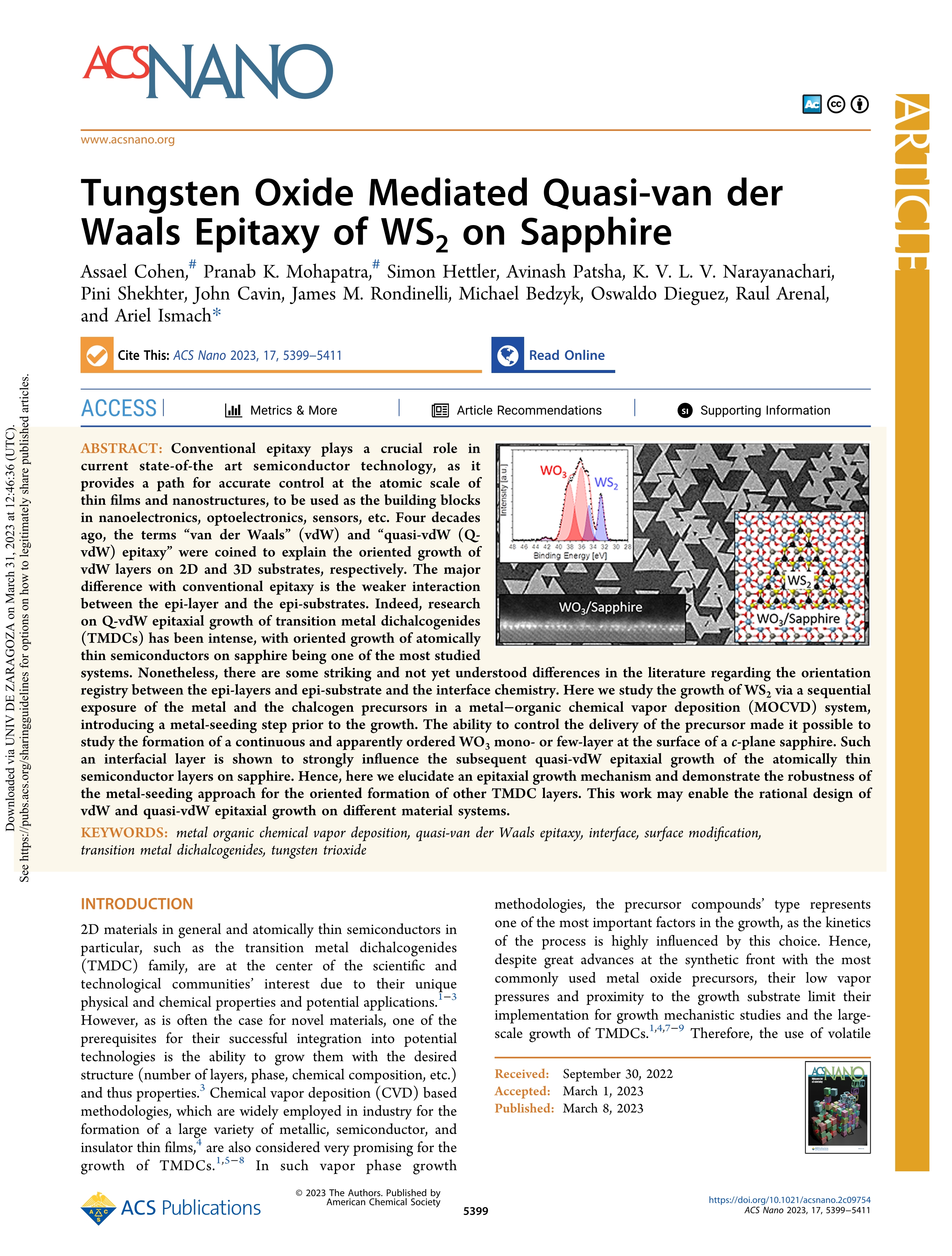
Resumen: Conventional epitaxy plays a crucial role in current state-of-the art semiconductor technology, as it provides a path for accurate control at the atomic scale of thin films and nanostructures, to be used as the building blocks in nanoelectronics, optoelectronics, sensors, etc. Four decades ago, the terms “van der Waals” (vdW) and “quasi-vdW (Q-vdW) epitaxy” were coined to explain the oriented growth of vdW layers on 2D and 3D substrates, respectively. The major difference with conventional epitaxy is the weaker interaction between the epi-layer and the epi-substrates. Indeed, research on Q-vdW epitaxial growth of transition metal dichalcogenides (TMDCs) has been intense, with oriented growth of atomically thin semiconductors on sapphire being one of the most studied systems. Nonetheless, there are some striking and not yet understood differences in the literature regarding the orientation registry between the epi-layers and epi-substrate and the interface chemistry. Here we study the growth of WS2 via a sequential exposure of the metal and the chalcogen precursors in a metal–organic chemical vapor deposition (MOCVD) system, introducing a metal-seeding step prior to the growth. The ability to control the delivery of the precursor made it possible to study the formation of a continuous and apparently ordered WO3 mono- or few-layer at the surface of a c-plane sapphire. Such an interfacial layer is shown to strongly influence the subsequent quasi-vdW epitaxial growth of the atomically thin semiconductor layers on sapphire. Hence, here we elucidate an epitaxial growth mechanism and demonstrate the robustness of the metal-seeding approach for the oriented formation of other TMDC layers. This work may enable the rational design of vdW and quasi-vdW epitaxial growth on different material systems.
Idioma: Inglés
DOI: 10.1021/acsnano.2c09754
Año: 2023
Publicado en: ACS NANO 17, 6 (2023), 5399-5411
ISSN: 1936-0851
Factor impacto JCR: 15.8 (2023)
Categ. JCR: CHEMISTRY, PHYSICAL rank: 14 / 178 = 0.079 (2023) - Q1 - T1
Categ. JCR: NANOSCIENCE & NANOTECHNOLOGY rank: 11 / 141 = 0.078 (2023) - Q1 - T1
Categ. JCR: CHEMISTRY, MULTIDISCIPLINARY rank: 15 / 231 = 0.065 (2023) - Q1 - T1
Categ. JCR: MATERIALS SCIENCE, MULTIDISCIPLINARY rank: 27 / 439 = 0.062 (2023) - Q1 - T1
Factor impacto CITESCORE: 26.0 - Engineering (all) (Q1) - Materials Science (all) (Q1) - Physics and Astronomy (all) (Q1)
Factor impacto SCIMAGO: 4.593 - Engineering (miscellaneous) (Q1) - Physics and Astronomy (miscellaneous) (Q1) - Nanoscience and Nanotechnology (Q1) - Materials Science (miscellaneous) (Q1)
Financiación: info:eu-repo/grantAgreement/ES/DGA/E13-20R
Financiación: info:eu-repo/grantAgreement/EC/H2020/823717/EU/Enabling Science and Technology through European Electron Microscopy/ESTEEM3
Financiación: info:eu-repo/grantAgreement/EC/H2020/889546/EU/Properties of nanomaterials made from misfit-layered compounds revealed by electron microscopy and simulations/PROMISES
Financiación: info:eu-repo/grantAgreement/ES/MICINN-AEI/PID2019-104739GB-I00/AEI-10.13039-501100011033
Tipo y forma: Artículo (Versión definitiva)
Área (Departamento): Área Física Materia Condensada (Dpto. Física Materia Condensa.)
 Debe reconocer adecuadamente la autoría, proporcionar un enlace a la licencia e indicar si se han realizado cambios. Puede hacerlo de cualquier manera razonable, pero no de una manera que sugiera que tiene el apoyo del licenciador o lo recibe por el uso que hace.
Exportado de SIDERAL (2024-11-22-12:00:46)
Visitas y descargas
Idioma: Inglés
DOI: 10.1021/acsnano.2c09754
Año: 2023
Publicado en: ACS NANO 17, 6 (2023), 5399-5411
ISSN: 1936-0851
Factor impacto JCR: 15.8 (2023)
Categ. JCR: CHEMISTRY, PHYSICAL rank: 14 / 178 = 0.079 (2023) - Q1 - T1
Categ. JCR: NANOSCIENCE & NANOTECHNOLOGY rank: 11 / 141 = 0.078 (2023) - Q1 - T1
Categ. JCR: CHEMISTRY, MULTIDISCIPLINARY rank: 15 / 231 = 0.065 (2023) - Q1 - T1
Categ. JCR: MATERIALS SCIENCE, MULTIDISCIPLINARY rank: 27 / 439 = 0.062 (2023) - Q1 - T1
Factor impacto CITESCORE: 26.0 - Engineering (all) (Q1) - Materials Science (all) (Q1) - Physics and Astronomy (all) (Q1)
Factor impacto SCIMAGO: 4.593 - Engineering (miscellaneous) (Q1) - Physics and Astronomy (miscellaneous) (Q1) - Nanoscience and Nanotechnology (Q1) - Materials Science (miscellaneous) (Q1)
Financiación: info:eu-repo/grantAgreement/ES/DGA/E13-20R
Financiación: info:eu-repo/grantAgreement/EC/H2020/823717/EU/Enabling Science and Technology through European Electron Microscopy/ESTEEM3
Financiación: info:eu-repo/grantAgreement/EC/H2020/889546/EU/Properties of nanomaterials made from misfit-layered compounds revealed by electron microscopy and simulations/PROMISES
Financiación: info:eu-repo/grantAgreement/ES/MICINN-AEI/PID2019-104739GB-I00/AEI-10.13039-501100011033
Tipo y forma: Artículo (Versión definitiva)
Área (Departamento): Área Física Materia Condensada (Dpto. Física Materia Condensa.)
Exportado de SIDERAL (2024-11-22-12:00:46)
Enlace permanente:
Visitas y descargas
Este artículo se encuentra en las siguientes colecciones:
Artículos > Artículos por área > Física de la Materia Condensada
Registro creado el 2023-04-20, última modificación el 2024-11-25